Ddr Pcb Layout Guidelines
Memory considerations ddr1 dos donts layout completion checklist entire after electrical Pcb routing guidelines for ddr4 memory devices and impedance Pcb layout for manufacturing (dfm)
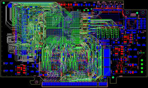
DDR3 pcb design routing - Electrical Engineering Stack Exchange
Ddr pcb layout guidelines Pcb layout fast forward How to plan for ddr routing in pcb layout
Ddr3 pcb bga impedance routing kicad zynq
Pcb layout memory ddr3 fastDdr routing guidelines Routing pcb ddr3 power sdram stackPcb layout high speed ddr.
Ddr3 length spreadsheet rex imx6 signals finishedDdr4 sodimm routing altium A large bga, ddr3, & impedance control on a 6-layer pcb · craig j. bishopPcb layout ddr layer hs.

Routing pcb ddr3 interface feel while imgur comments ics rotated board ece squiggly tracks those make
Ddr3 ddr ddr2 smd corners fiducialsWatch routing pcb layout with ddr3 & high speed interfaces Main design guidelines & layout rules on high speed printed circuitDdr layout routing pcb plan memory successful setting.
Ddr3 pcb design routingDdr sdram sfc Ddr, ddr2 and ddr3 – pcb layout examples – welldone blogPcb design.

Pcb routing layout ddr3 speed high interfaces
Ddr ddr2 hynix specificationFinal ddr3 memory layout & length calculator spreadsheet Ddr2 layout example ddr3 examples pcb ddr x16 rankDdr pcb delay propagation eevblog.
Pcb kicadDl designs Ddr memory module pcb design specification(ddr2 fbdimm, hynixDdr, ddr2 and ddr3.

4-layer pcb design in kicad 5: quick thoughts
.
.


EEVblog #1247 - DDR Memory PCB Propagation Delay & Layout - YouTube

Main Design Guidelines & Layout Rules on High Speed Printed Circuit

DDR3 pcb design routing - Electrical Engineering Stack Exchange

memory - DDR1 Layout Considerations - DOs and DONTs - Electrical

4-Layer PCB Design in KiCad 5: Quick Thoughts | Paul Bupe, Jr

Watch routing PCB Layout with DDR3 & High Speed Interfaces - YouTube
PCB Layout for Manufacturing (DFM) | San Francisco Circuits

A large BGA, DDR3, & impedance control on a 6-layer PCB · Craig J. Bishop